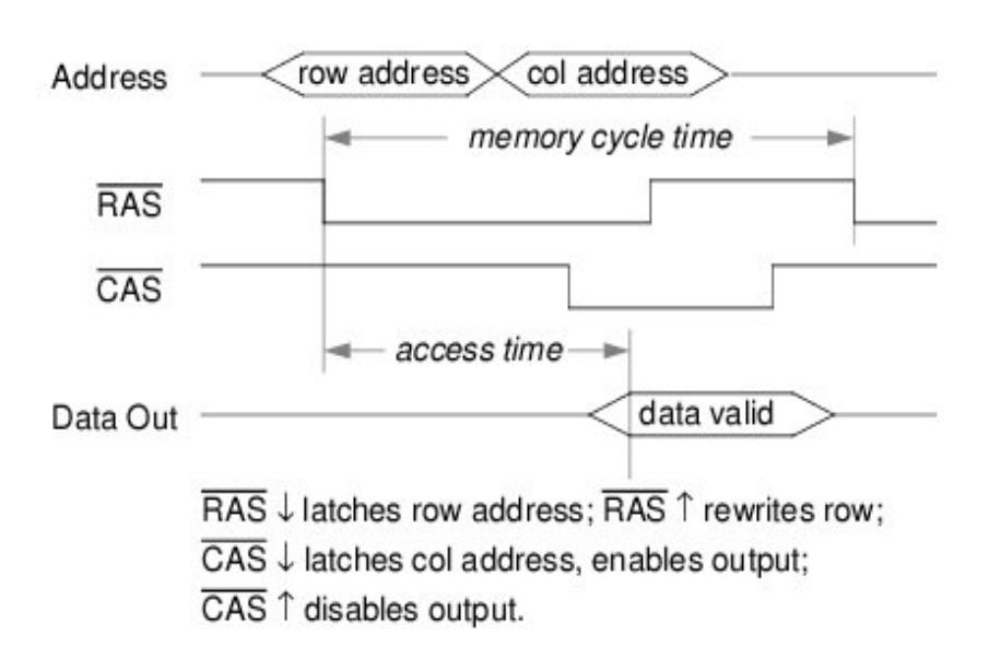
Page Mode DRAM
A DRAM bank is a 2D array of rows * columns
A “DRAM row” is also called a “DRAM page”
“Sense amplifiers” also called “row buffer”
Each address is a <row, column> pair
DRAM Access :
Access to a “closed row”
Activate command opens row (placed in row buffer)
Read/Write command reads /writes column in the row buffer
Pre-charge command closes the row and prepares the bank for next access
Access to an “open row“
No need for activate command
Addressing:
By specifying row and column addresses sequentially
Requires separate row_address_strobe (RAS) & column_addr_strobe (CAS)
Cycle types:
random read, random write
fast page mode read, fast page mode write
CBR refresh (CAS before RAS)
“hidden” refresh
read/modify/write
High performance DRAM cycles
Optimizations to get more bits per RAS
Nibble mode (1 nibble == 4 sequential bits or cells)
present RAS, then CAS, CAS, CAS, CAS
Fast page mode
present RAS, then provide col addr, then CAS
then change to different column addr (within same row), then CAS again ...
Static column
present RAS, then column address and CAS
then change column addr (like an SRAM) without cycling CAS
Some history:
The addressing optimizations helped improve performance in first and second generation DRAMs. Post, this single bank performance was saturated.
SDRAM : Synchronous DRAM
Third generation DRAM
Made by adding a synchronous interface between the basic core DRAM operation/circuitry of second-generation DRAMs and the control coming from off-chip to make the DRAM operation faster
All commands and operations to and from the DRAM are executed on the rising edge of a master or command clock signal
Additionally, the memory is segmented into banks
The bank selected is determined by the addresses BA1 and BA0
Advantages of banked SDRAM
Possible to activate a row in one bank and then, while the row is opening, perform an operation in some other bank (such as reading or writing)
In addition, one of the banks can be in a PRECHARGE mode (the bitlines are driven to Vcc/2) while accessing one of the other banks and, thus, in effect hiding PRECHARGE and allowing data to be continuously written to or read from the SDRAM.
Double Data Rate Synchronous Dynamic Random Access Memory or DDR SDRAM
The interface uses double pumping (transferring data on both the rising and falling edges of the clock signal) to lower the clock frequency
One advantage of keeping the clock frequency down is that it reduces the signal integrity requirements on the circuit board connecting the memory to the controller
The name "double data rate" refers to the fact that a DDR SDRAM with a certain clock frequency achieves nearly twice the bandwidth of a SDR SDRAM running at the same clock frequency, due to this double pumping
There have been several generations of DDR now with optimizations in the hierarchy and addressing. Some use-cases like Video (VRAM) and embedded (LPDDR) have specialized DDRs.
A DRAM Chip
contains multiple banks (8 common these days)
banks share command/address/data buses
The chip itself has narrow interface (4-16 bits per read)
DRAM Rank and Module
Rank: Multiple chips operate together to form a wide interface
All chips comprising a rank are controlled at the same time
Respond to a single command
Share address and command buses, but provide different data
A DRAM module consists of one or more ranks
Eg. DIMM (Dual inline memory module)
This is what you plug into your motherboard
Advantages of a DIMM
Acts as a high capacity DRAM chip with a wide interface
Flexibility: Memory controller does not need to deal with individual chips
Disadvantages
Granularity: Accesses cannot be smaller than the interface width
Multiple DIMMs:
Advantages
Enables even higher capacity
Disadvantages
interconnect complexity and energy consumption can be high
The Role of the Memory Controller and Channels
The memory controller is a critical component that manages the flow of data between the CPU and the DRAM. It issues commands to the DRAM, such as activate, read, write, and pre-charge, to facilitate data access. The memory controller also handles the timing and sequencing of these commands to ensure efficient data transfer.
Memory controllers can define channels to manage data flow:
Independent Channels: Utilize two memory controllers for separate data paths, allowing for parallel data processing.
Dependent/Lockstep Channels: Use one memory controller with a wide interface for synchronized data access, ensuring data integrity and consistency. We can have channels(defined by memory controller.
Some of my favorite material on this DDR hierarchy and addressing:
https://www.systemverilog.io/design/ddr4-basics/
https://www.systemverilog.io/design/lpddr5-tutorial-physical-structure/


